3 to 8 Decoder using Verilog Programming
Content to be covered :
- Decoder -> what is it?
- Truth Table
- Enable logic
- Verilog Code
- RTL view
- Testbench
- Stimulation
1. Decoder -> what is it?

A decoder is a digital circuit, that helps convert an given n coded input to a 2n outputs.
A decoder various applications such as data multiplexing and data demultiplexing, seven segment displays, and as address decoders for memory and port-mapped I/O.
There are few different types of decoders. For example, the above is 1-of-n type of binary decoder, meaning that when, an input is given only 1 or none of the output is activated.
A binary decoder is usually implemented as a standalone IC or as a part of more complex ICs.
So, if there are N inputs, the decoder will produce a maximum of 2n outputs. Thus, if we have 3-bit input we will have 23 = 8-bit output. In Verilog Coding, of a particular combinational circuit it is necessary to know the number of input/output a particular chip may require.
Since, we now understand the concept behind the decoder, we should start with the logic oriented part.
2. Truth Table
Any digital circuit can be realized using Truth Table. This is the beauty of digital Electronics. Also using this table to simplify the logic of the design we initially thought off.
| DIN | DOUT |
|---|---|
| 000 | 00000001 |
| 001 | 00000010 |
| 010 | 00000100 |
| 011 | 00001000 |
| 100 | 00010000 |
| 101 | 00100000 |
| 110 | 01000000 |
| 111 | 10000000 |
3. Enable Logic
Yes, the theoretical part of the design is almost over with the understanding of the enable input, which is the driver of the combinational logic. Take a look at the transformed truth table
| Enable | DIN | DOUT |
|---|---|---|
| 1 | XXX | 00000000 |
| 0 | 000 | 00000001 |
| 0 | 001 | 00000010 |
| 0 | 010 | 00000100 |
| 0 | 011 | 00001000 |
| 0 | 100 | 00010000 |
| 0 | 101 | 00100000 |
| 0 | 110 | 01000000 |
| 0 | 111 | 10000000 |
You can see that the design modifies in a sense that if the enable is logic 0 => the output becomes zero no matter the input. Thus, this enable can be used as a switch by many devices in order to keep this device “on” only in the time of need. Also, this type of enabling is called active low, since the chip gets activated when the enable turns low(i.e. enable = 0).
4. Verilog Code
Okay so without further delay, here’s the code for decoder.
Also here is the link to my git repo -> https://github.com/nirbhay12345/chipDesign/Decoder
module Decoder ( // 3 to 8 decoder
    input [2:0] din, // input signal
    input enable, // chip enable signal => active low
    output reg [7:0] dout // selected output
);

    // main logic
    always @* begin
        if (enable)
            dout[7:0] <= 8'h00;
        else
            case (din[2:0])
                3'b000 : dout[7:0] <= 8'h01;
                3'b001 : dout[7:0] <= 8'h02;
                3'b010 : dout[7:0] <= 8'h04;
                3'b011 : dout[7:0] <= 8'h08;
                3'b100 : dout[7:0] <= 8'h10;
                3'b101 : dout[7:0] <= 8'h20;
                3'b110 : dout[7:0] <= 8'h40;
                3'b111 : dout[7:0] <= 8'h80;
                //default is necessary to avoid any latchs
                default: dout[7:0] <= 8'h00;
            endcase
    end

endmodule
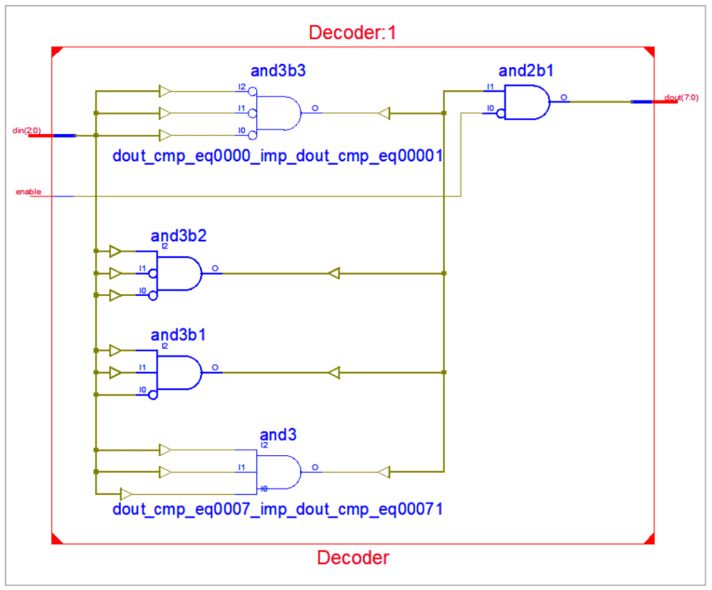
5. RTL view
The design thus converted into a simple combinational logic. Also, you can always convert it into a parametric form in order to scale things up. But that’s up to you to decide.
6. Testbench
Here is the testbench :
module Decoder_tb;
    reg [2:0] din;
    reg enable;
    wire [7:0] dout;

    // instantiate the design block
    Decoder d1(din, enable, dout);

    integer i;

    initial begin
        enable = 1'b1;
        din = 3'b000;
        i = 0;
        #100
        enable = 1'b0;
        for (i = 0; i < 8; i=i+1) begin
            din = din + 3'b001;
            #100;
        end
    end

endmodule
The above testbench probably includes all the possibility of the design and thus completes our design. Just one thing to Go -> Stimulation.
7. Stimulation
Time to test and observe our design.
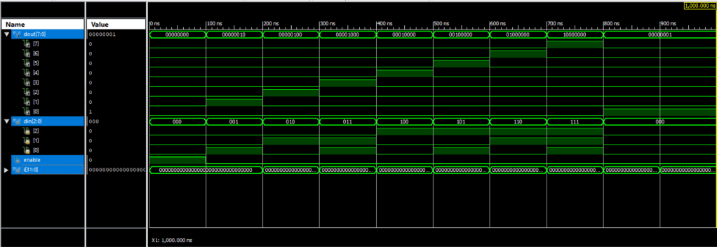
Great going !! We now have a decoder of our own! 😎