
Verilog Programming
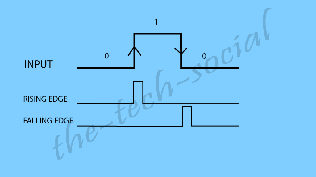
Edge detectors can be realized using many circuits in digital electronics. Here we will try to create a dual edge detector using FSM(Finite state Machine).
Basically, we are trying to detect the rising as well as falling edges of the input signal. These type of designs are important when our application is event driven or where we need to validate the data transfer, etc.
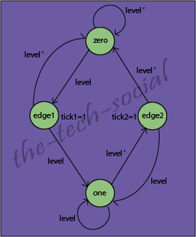
FSM chart:
There are two types of FSM :
- Moore based FSM
- Mealy Based FSM
Basically, in Moore based design the output depends only on the current state of the state register, while in Mealy Based design the output depends on both the current state as well as the input logic.
Anyway, the concept of FSM demands a completely new series of blogs which I’ll be working on soon.
Here, in this above example we can clearly see the logic flow of the FSM chart.
Verilog Code:
The code is divided into three different parts
- next-state logic
- state register
- output logic
module dual_edge_detector (
    input wire clk, reset,
    input wire level, // input signal
    output reg tick1, tick2// the alert signals for rising and falling edge resp.
);
    // all states of the state machine
    localparam [1:0] zero=2'b00, edge1=2'b01, edge2=2'b10, one=2'b11;

    // register required in the FSM
    reg [1:0] state_next, state_reg;

    // state register
    always @(posedge clk, posedge reset)
        if(reset)
            state_reg <= zero;
        else
            state_reg <= state_next;

    // next state logic and output logic
    always @* begin
        // default values
        state_next = state_reg;
        tick1 = 1'b0;
        tick2 = 1'b0;
        case (state_reg)
            zero :
                if (level) begin
                    state_next = edge1;
                    tick1 = 1'b1;
                end
                else
                    state_next = zero;
            edge1 :
                if (level)
                    state_next = one;
                else
                    state_next = zero;
            one :
                if (~level) begin
                    state_next = edge2;
                    tick2 = 1'b1;
                end
                else
                    state_next = one;
            edge2 :
                if (level)
                    state_next = one;
                else
                    state_next = zero;
            default: state_next = zero;
        endcase
    end
endmodule
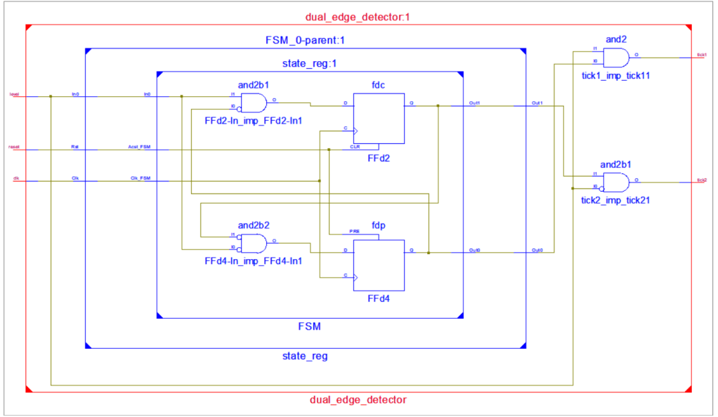
RTL view
Testbench
Apparently, there are many ways of writing a testbench for such a design. Here, I have tried to write a version, however it is not all, you can always come up with a better testbench and improve the design.
module dual_edge_tb;
    reg clk;
    reg reset;
    reg level;
    wire tick1, tick2;

    // instantiate the design
    dual_edge_detector d1(.clk(clk),
                          .reset(reset),
                          .level(level),
                          .tick1(tick1), .tick2(tick2));

    // initialize the clock
    initial clk = 1'b0;

    always #20 clk = ~clk;

    initial begin
        reset = 1'b1; level = 1'b0;
        #35 reset = 1'b0; level = 1'b0;
        #115 level = 1'b1;
        #90 level = 1'b0;
        #80 level = 1'b1;
        #90 level = 1'b0;
        #80 level = 1'b1;
        #100 level = 1'b0;
    end

endmodule
Stimulation
This is the stimulation of the following design with the give testbench.

Here, we can see that the tick1 goes high when the design detects a transition from zero to one, whereas the tick2 goes high when the design detects a transition from one to zero.
Great!!😎😎
