
Full adder using Verilog and Isim stimulation.
Concepts covered in the blog :
Half adder
If you are reading this blog, then you are probably familiar with digital electronics. If not then here is some basic on full adder what it is and why we need it, if yes then this might be a quick revision for you all.
So what is a full adder? before that we need to know what is a half adder.
Basically, half adder is a digital circuit which adds two bits. It is the simplest form of a adder circuit.
Let us take that bits to be A and B. Thus what the half adder digital circuit does is that, it generates a Sum and Carry according to the given input.
| A | B | Sum | Carry |
| 0 | 0 | 0 | 0 |
| 0 | 1 | 1 | 0 |
| 1 | 0 | 1 | 0 |
| 1 | 1 | 0 | 1 |
Thus, from the truth table we can infer the following Boolean equations :

A ⊕ B = Sum
A . B = Carry
Thus, we can easily obtain the above visualization of half adder.
Full adder -> Concept
Half adder is good enough but the tricky part begins when we switch to addition of more than one bit. Yes, you guessed it right.
In addition of more than two bits, we need to consider the Carry that is generated by the LSB (Least Significant Bit), or to say the bit having a lesser place value.
Here, full adder comes into picture. the full adder also takes into consideration the carry of the previous bit, increasing one input in the circuit, this might be more clear by seeing the truth table and then visualizing the full adder.
| A | B | Cin | Sum | Cout |
| 0 | 0 | 0 | 0 | 0 |
| 0 | 0 | 1 | 1 | 0 |
| 0 | 1 | 0 | 1 | 0 |
| 0 | 1 | 1 | 0 | 1 |
| 1 | 0 | 0 | 1 | 0 |
| 1 | 0 | 1 | 0 | 1 |
| 1 | 1 | 0 | 0 | 1 |
| 1 | 1 | 1 | 1 | 1 |

Sum = A ⊕ B ⊕ Cin
Cout = A.B + Cin(A ⊕ B)
Thus, by now you might be clear about what a half adder and full adder does and comprises off.
Now, to answer the question -> how can you create actual hardware, using the HDL language like Verilog?
Verilog Code
Verilog is one of the languages used to describe hardware, hence the name -> HDL (Hardware Description Language).
You might need a tool like -> Xilinx ISE design suite or others to create the following. Better to check you have installed everything.
module adder_carry(
    input wire [3:0] i_a, i_b,
    output wire [3:0] o_sum,
    output wire o_cout
    );

	wire [4:0] int_sum;

	assign int_sum = {1'b0, i_a} + {1'b0, i_b};
	assign o_sum = int_sum[3:0];
	assign o_cout = int_sum[4];

endmodule
The above code represents a 4-bit full adder Verilog code.
The 5th bit of the int_sum variable is taken to represent the carry generated from MSB of the addition of i_a and i_b signals.
RTL view
The RTL view is generated by the tool you are using automatically, by just synthesizing the code.
It has predefined hardware for a particular code and the tool then converts your written code into actual hardware schematic.
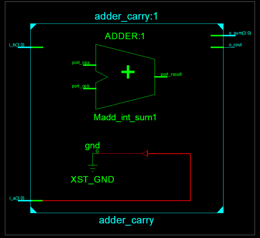
The above given is the RTL view of the code written above. It is necessary to understand that through Verilog we are trying to create a hardware and thus the RTL view helps us to visualize the hardware schematic before it can be further evaluated.
Also, RTL view helps us to see what does the hardware comprises of and gives us a digital circuit insight for further understanding of the hardware.
Different methods in Verilog may give different hardware approaches, thus the choice of hardware customization entirely depends over the designer and the methods he/she may use.
Finally, our goal is to make systems with the most efficient yet with reasonable hardware, where the trade-off between the hardware and the speed of execution of a particular task plays an important role.
Stimulation (ISIM)
The stimulation of a given circuit further helps us to understand the response of the circuit in dynamic conditions. Thus, helping us to know the in’s and out’s of the circuit.
This helps in visualization of the circuit response and also rectifies for any error that our system may possess.
The Stimulation of the above Verilog code is given below.

The result is as expected.
Wish you a happy learning!!
