Since we have learned to make full adder as well as half adder, we now can make a N-bit adder which is a scalable version of adder.
This is a more practical approach to making an adder, since the Full Adder and Half Adder are building blocks of this module.
If you do not know how to make a full or half adder please do visit this below link, to clear basic concepts of adders
https://techno10.tech.blog/2020/10/06/verilog-programming/
Concepts to be covered
- Understanding the N-bit adder
- Instantiating a module in another module
- RTL view (what does for loop mean in Verilog)
- Writing testbench for our adder: covering the edge cases
- Analyzing the output : Stimulation
1. Understanding the N-bit adder
The adder is one of the most fundamental part of any digital circuit, yet it is inefficient if used as just the base forms i.e. as full adder and half adder.
As these only add one bit at a time, while in reality we need a lot more than that to occur simultaneously.
So, we combine the functionality of both the adders and put it together to build a more practical approach -> N-bit Adder.
Since we have a parameter N, we can scale it up to as many bits as we need to.
A N-bit adder can be made by using:
- 1 half bit adder
- N-1 full bit adder
A 4-bit adder using 3-full adder and 1-half adder
The above is the example of the 4-bit adder using one half bit and three full bit adders.
2. Instantiating modules in another module
We can use our already ready code for the half and full adder to make the new N-bit Adder, by simply instantiating the modules in our new module.
// the tech social -> Verilog Programming
// half adder module
module half_adder (
    input a, b,
    output sum, carry
);
    assign sum = a ^ b;   // sum of half adder
    assign carry = a & b; // carry of half adder

endmodule

// the tech social -> Verilog Programming
// full adder module
module full_adder (
    input a, b, cin,
    output sum, cout
);
    assign sum = a ^ b ^ cin;
    assign cout = (a & b) | (cin & (a ^ b));

endmodule

// the tech social -> Verilog Programming
// N-bit adder module
// here let N = 8 => 8-bit adder
module N_bit_adder
#(parameter N = 8)
(
    input [N-1:0] input1, input2,
    output [N-1:0] answer
);
    wire [N-1:0] carry;// intermediate carry outputs
    wire carry_out;// for the end carry output
    genvar i;// general variable

    generate
      for (i = 0; i < N; i = i + 1) begin: generate_N-bit_adder
        if (i == 0) // LSB bit adder
          half_adder b(input1[0], input2[0], answer[0], carry[0]);
        else // rest all adders
          full_adder b(input1[i], input2[i], carry[i-1], answer[i], carry[i]);
      end

        assign carry_out = carry[N-1];
    endgenerate
endmodule
We can see that we generate half adder only for the LSB adder and other are all Full adders. We accomplish this with the help of simple for loop followed by if-else condition.
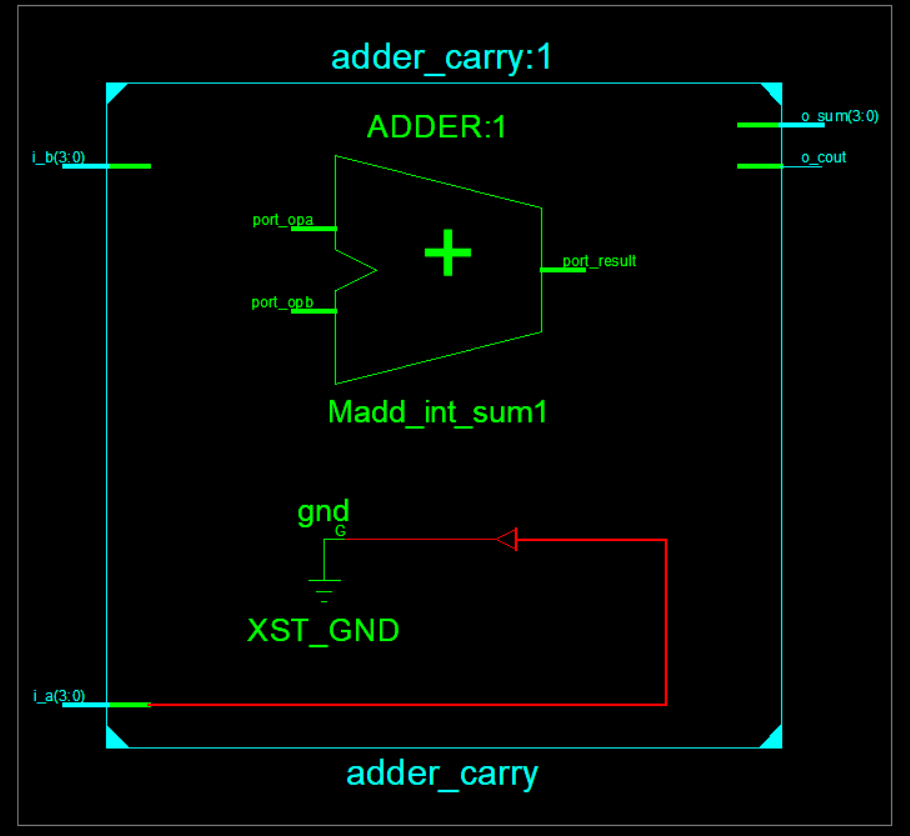
3. RTL View (what does for loop mean in Verilog)
Here you can see the “for loop” works differently than it works in C or C++.
Yes you got that right, here it generates hardware using synthesis tools. Which means the number of times we instantiate the full adder through the for loop, it generates the full adder hardware the respective number of times.
To put it simply we can directly look at the RTL view of the module.

It seems we are close enough to the verification of our module now!!
4. Writing testbench for our adder: covering the edge cases
Testbench turns out to be the most critical part of any chip design since it is this process which sets apart a good design from a bad one.
Writing the test bench for this n-bit adder however is quite easy, and simply involves the knowledge of addition in binary numbers.
Since, the adder we designed will be able to add 8 bits we can play around some possibilities such as 256 + 1, – 2 – 4, etc. The following test bench might be sufficient as per this module.
Also here is my git repo for the N-bit adder code -> https://github.com/nirbhay12345/chipDesign/N-bit_adder
//the tech social
// testbench for N-bit(in this case 8-bit) adder
module N_bit_adder_tb;
    // parameter N = 8;
    reg [7:0] i1, i2;
    wire [7:0] answer;

    // initialization of the design block
    N_bit_adder uut(.input1(i1), .input2(i2), .answer(answer));

    initial begin
        i1 = 230;
        i2 = 10;
        #100;
        i1 = 256;
        i2 = 1;
        #100;
        i1 = -1;
        i2 = -3;
        #100;
        i1 = 100;
        i2 = 200;
        #100;
        i1 = 30;
        i2 = 70;
        #100;
        i1 = 2;
        i2 = -255;
        #100;
    end

endmodule
5. Analyzing the output : Stimulation
This is were we learn our designs capability :

Okay so we have successfully achieved our goal. 😎