Encoder using – Verilog

Encoders are digital circuits that are used to encode data, and convert human understandable data to machine understandable data.

A simple example is ASCII encoder, which converts the key pressed on the key board to its corresponding, machine understandable, code.

Encoders are very useful in digital circuits, from pocket calculators to keyboards and much more.

Here we are going to build a simple “priority encoder” using Verilog.

Block diagram
<p value="<amp-fit-text layout="fixed-height" min-font-size="6" max-font-size="72" height="80">The realization of encoder is as simple as it looks. But first we need to understand it in terms of truth table and then minimize the logic function. After that we will have the minimalistic logic to implement.The realization of encoder is as simple as it looks. But first we need to understand it in terms of truth table and then minimize the logic function. After that we will have the minimalistic logic to implement.

D7D6D5D4D3D2D1D
10000000
01000000
00100000
00010000
00001000
00000100
00000010
00000001
INPUTS
Y2Y1Y0
111
110
101
100
011
010
001
000
OUTPUTS

The above is the respective outputs produced by the encoder when any one of the lines is kept high.

The above design can generate error when there are more than one lines that are kept high. This is the major drawback of a simple encoder.

In order to prevent this error, we can introduce priority of inputs. This can be achieved if we discard a Logic High input after one is received in the priority order.

This can be simply understood by redrawing the Truth Table.

D7D6D5D4D3D2D1D0
1XXXXXXX
01XXXXXX
001XXXXX
0001XXXX
00001XXX
000001XX
0000001X
00000001
INPUTS
Y2Y1Y0
111
110
101
100
011
010
001
000
OUTPUTS

This above method has an advantage over the simple encoder, that it gives priority order to the input lines. Thus, if more than two lines are high, only the one with highest priority will be considered.

Now writing Code for this is fairly simple:

Code :

// the-tech-social
// Priority Encoder
// this is a 8 to 3 decoder => with priority enabled
module priority_encoder(
    input wire[7:0] in, // input given
    input wire enable, //chip enable => active high
    output reg [2:0] y // encoded output
    );
	
    always@ * begin
       if (!enable)
         y[2:0] = 4'h0;
       else
         casez(in)
            8'b1???????: y = 3'b111; // d7
            8'b01??????: y = 3'b110; // d6
            8'b001?????: y = 3'b101; // d5
            8'b0001????: y = 3'b100; // d4
            8'b00001???: y = 3'b011; // d3
            8'b000001??: y = 3'b010; // d2 
            8'b0000001?: y = 3'b001; // d1
            8'b00000001: y = 3'b000; // d0
            default: y = 3'b111;     // default is highest priority => d7
	 endcase
    end
endmodule

You can see that I have also added an active high enable in the above code for chip enable. So, when the enable is low no output is received.
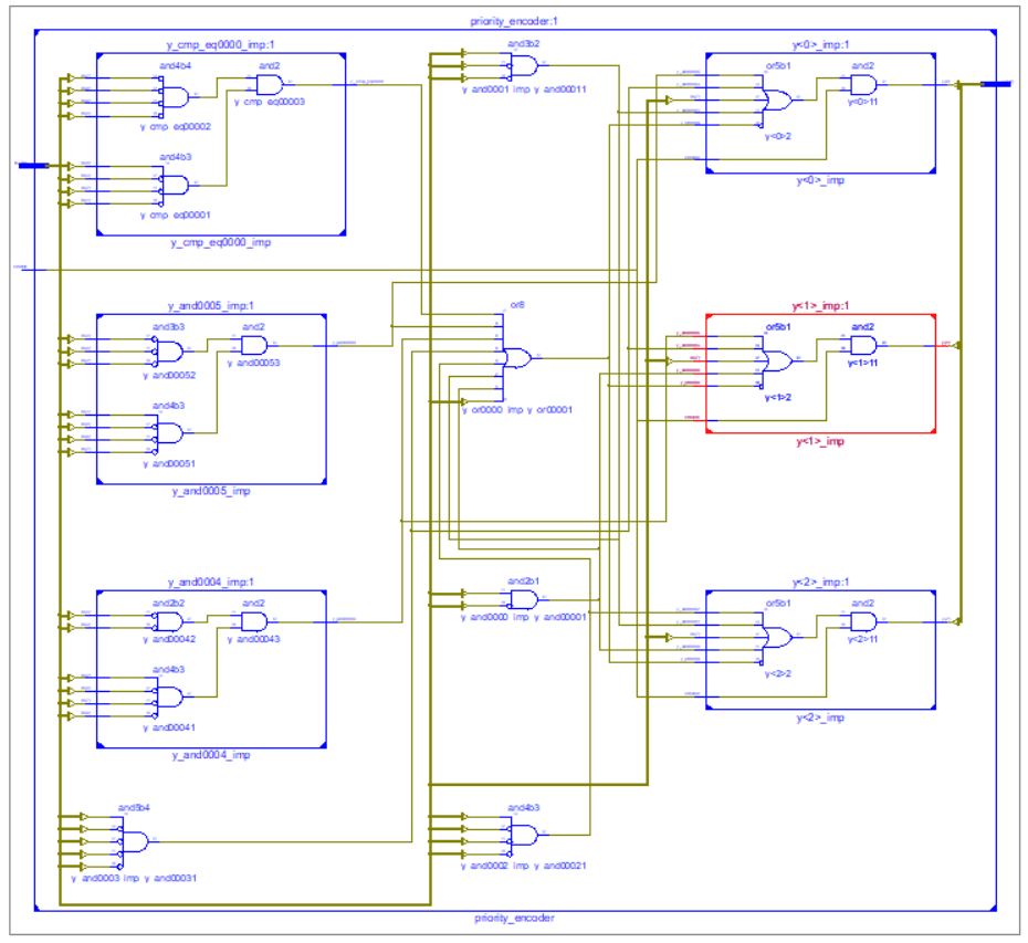
RTL view:

The following RTL view is generated using this code,

Generated using Xilinx ISE

Testbench:

Yes, after RTL generation we generally try to figure out a testbench. But since we have already tried a decoder, why not try to link these together.

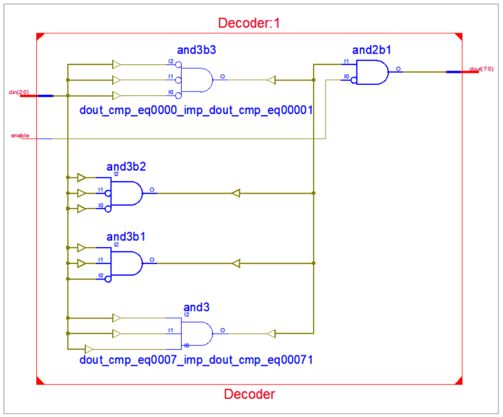
If you are wondering where is the decoder, please take a look here: https://techno10.tech.blog/2020/12/18/decoder-using-verilog/

Now then, if we need to test the encoder, we can give the inputs at the encoder end and when the output is generated, we can get these to connect to the inputs of the decoder, which in turn will generate the input that we first choose to give in.

What I mean can be shown using the below code:

// the-tech-social
// Test_encoder module
// input => encoder => decoder => output
module Test_encoder (
    input wire[7:0] in, // input given
    input wire enable, //chip enable => active high
    output wire [7:0] out 
);

    wire [2:0] inter;
    // 8to3 encoder module instantiation
    priority_encoder e1(.in(in), .enable(enable), .y(inter));
    // 3to8 decoder module instantiation 
    Decoder d1(.din(inter), .enable(~enable), .dout(out));
    
endmodule

We can see that the intermediate wire “inter” that stores the value of the encoder is then given as the input to the decoder. Also, the enable is connected “inverted” with the decoder since it is active low and “normally” with the encoder since it is active high.

Just remember that we have used 8to3 encoder and 3to8 decoder here to achieve the objective.

This can also be seen in the below RTL view of the module.

Encoder-Decoder test module

Now we can write a test bench to this and expect the output to be the input given as simple as that.

Code for test bench:

// the-tech-social
// Test_encoder_tb
// Testbench for Test_encoder
module Test_encoder_tb;
    reg [7:0] in;
    reg enable;
    wire [7:0] out;

    // initializing the design
    Test_encoder t1(in, enable, out);

    integer i;

    initial enable = 1'b1;

    initial begin
        in = 00000001;
        i = 0;
        #100;
        for (i = 0; i < 8; i=i+1) begin
           in = in<<1;
           #100; 
        end
    end
endmodule

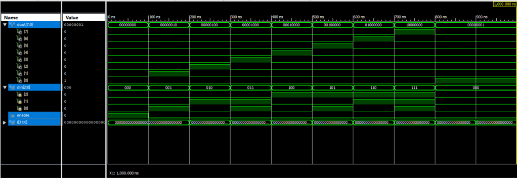
This sure is fun, and we can see the output following the input in the stimulation waveform.

Stimulation:

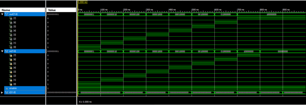
Here, we can observe that the last input is ‘00000000’ yet the output is ‘10000000’. This is something I will let you figure out by yourself, and fix so that you can have a proper understanding of the encoder and decoder that we have used here.

So, now we have a encoder and a circuit to test its functionality.

Great!!!😎😎

Advertisement

FSM Based Dual Edge Detector

Verilog Programming

Edge detector waveform

Edge detectors can be realized using many circuits in digital electronics. Here we will try to create a dual edge detector using FSM(Finite state Machine).

Basically, we are trying to detect the rising as well as falling edges of the input signal. These type of designs are important when our application is event driven or where we need to validate the data transfer, etc.

FSM chart:

Moore based FSM Chart for dual edge detector

There are two types of FSM :

  • Moore based FSM
  • Mealy Based FSM

Basically, in Moore based design the output depends only on the current state of the state register, while in Mealy Based design the output depends on both the current state as well as the input logic.

Anyway, the concept of FSM demands a completely new series of blogs which I’ll be working on soon.

Here, in this above example we can clearly see the logic flow of the FSM chart.

Verilog Code:

The code is divided into three different parts

  • next-state logic
  • state register
  • output logic
module dual_edge_detector (
    input wire clk, reset, 
    input wire level, // input signal
    output reg tick1, tick2// the alert signals for rising and falling edge resp.
);
    // all states of the state machine
    localparam [1:0] zero=2'b00, edge1=2'b01, edge2=2'b10, one=2'b11;

    // register required in the FSM
    reg [1:0] state_next, state_reg;

    // state register
    always @(posedge clk, posedge reset)
        if(reset)
            state_reg <= zero;
        else
            state_reg <= state_next;

    // next state logic and output logic
    always @* begin
        // default values
        state_next = state_reg;
        tick1 = 1'b0;
        tick2 = 1'b0;
        case (state_reg)
            zero : 
                if (level) begin
                    state_next = edge1;
                    tick1 = 1'b1;
                end
                else
                    state_next = zero;
            edge1 :
                if (level)
                    state_next = one;
                else
                    state_next = zero;
            one :
                if (~level) begin
                    state_next = edge2;
                    tick2 = 1'b1;
                end
                else
                    state_next = one;
            edge2 :
                if (level) 
                    state_next = one;
                else
                    state_next = zero;
            default: state_next = zero;
        endcase
    end
endmodule

RTL view

Generated using Xilinx ISE

Testbench

Apparently, there are many ways of writing a testbench for such a design. Here, I have tried to write a version, however it is not all, you can always come up with a better testbench and improve the design.

module dual_edge_tb;
    reg clk;
    reg reset;
    reg level;
    wire tick1, tick2;

    // instantiate the design
    dual_edge_detector d1(.clk(clk), 
                          .reset(reset), 
                          .level(level), 
                          .tick1(tick1), .tick2(tick2));

    // initialize the clock
    initial clk = 1'b0;

    always #20 clk = ~clk;

    initial begin
        reset = 1'b1; level = 1'b0;
        #35 reset = 1'b0; level = 1'b0;
        #115 level = 1'b1;
        #90 level = 1'b0;
        #80 level = 1'b1;
        #90 level = 1'b0;
        #80 level = 1'b1;
        #100 level = 1'b0;
    end

endmodule

Stimulation

This is the stimulation of the following design with the give testbench.

Generated using Xilinx ISE

Here, we can see that the tick1 goes high when the design detects a transition from zero to one, whereas the tick2 goes high when the design detects a transition from one to zero.

Great!!😎😎

Decoder Using – Verilog

3 to 8 Decoder using Verilog Programming

Content to be covered :

  • Decoder -> what is it?
  • Truth Table
  • Enable logic
  • Verilog Code
  • RTL view
  • Testbench
  • Stimulation

1. Decoder -> what is it?

A decoder is a digital circuit, that helps convert an given n coded input to a 2n outputs.

A decoder various applications such as data multiplexing and data demultiplexing, seven segment displays, and as address decoders for memory and port-mapped I/O.

There are few different types of decoders. For example, the above is 1-of-n type of binary decoder, meaning that when, an input is given only 1 or none of the output is activated.

A binary decoder is usually implemented as a standalone IC or as a part of more complex ICs.

So, if there are N inputs, the decoder will produce a maximum of 2n outputs. Thus, if we have 3-bit input we will have 23 = 8-bit output. In Verilog Coding, of a particular combinational circuit it is necessary to know the number of input/output a particular chip may require.

Since, we now understand the concept behind the decoder, we should start with the logic oriented part.

2. Truth Table

Any digital circuit can be realized using Truth Table. This is the beauty of digital Electronics. Also using this table to simplify the logic of the design we initially thought off.

DINDOUT
000 00000001
001 00000010
010 00000100
011 00001000
100 00010000
101 00100000
110 01000000
111 10000000
Truth Table for 3 to 8 decoder

3. Enable Logic

Yes, the theoretical part of the design is almost over with the understanding of the enable input, which is the driver of the combinational logic. Take a look at the transformed truth table

EnableDINDOUT
1XXX00000000
000000000001
000100000010
001000000100
001100001000
010000010000
010100100000
011001000000
011110000000
Truth Table for 3 to 8 decoder with enable

You can see that the design modifies in a sense that if the enable is logic 0 => the output becomes zero no matter the input. Thus, this enable can be used as a switch by many devices in order to keep this device “on” only in the time of need. Also, this type of enabling is called active low, since the chip gets activated when the enable turns low(i.e. enable = 0).

4. Verilog Code

Okay so without further delay, here’s the code for decoder.

Also here is the link to my git repo -> https://github.com/nirbhay12345/chipDesign/Decoder

module Decoder ( // 3 to 8 decoder
    input [2:0] din, // input signal
    input enable, // chip enable signal => active low
    output reg [7:0] dout // selected output
);

    // main logic
    always @* begin
        if (enable)
            dout[7:0] <= 8'h00;
        else
            case (din[2:0])
                3'b000 : dout[7:0] <= 8'h01;
                3'b001 : dout[7:0] <= 8'h02;
                3'b010 : dout[7:0] <= 8'h04;
                3'b011 : dout[7:0] <= 8'h08;
                3'b100 : dout[7:0] <= 8'h10;
                3'b101 : dout[7:0] <= 8'h20;
                3'b110 : dout[7:0] <= 8'h40;
                3'b111 : dout[7:0] <= 8'h80;
                //default is necessary to avoid any latchs
                default: dout[7:0] <= 8'h00; 
            endcase
    end

endmodule

5. RTL view

The design thus converted into a simple combinational logic. Also, you can always convert it into a parametric form in order to scale things up. But that’s up to you to decide.

Generated using Xilinx ISE

6. Testbench

Here is the testbench :

module Decoder_tb;
    reg [2:0] din;
    reg enable;
    wire [7:0] dout;

    // instantiate the design block
    Decoder d1(din, enable, dout);

    integer i;

    initial begin
        enable = 1'b1;
        din = 3'b000;
        i = 0;
        #100
        enable = 1'b0;
        for (i = 0; i < 8; i=i+1) begin
            din = din + 3'b001;
            #100;
        end
    end

endmodule

The above testbench probably includes all the possibility of the design and thus completes our design. Just one thing to Go -> Stimulation.

7. Stimulation

Time to test and observe our design.

Great going !! We now have a decoder of our own! 😎

Arithmetic & logical Unit – Verilog

Making a arithmetic and logical unit (ALU) using Verilog Programming

Here we are going to make a clock driven => synchronous ALU.

Content to be covered

  • ALU (Arithmetic & Logical Unit )
  • Data Bus & Instruction Bus
  • Introduction to clock concept => Synchronous design
  • Arithmetic unit
  • Logical unit
  • Combining the ALU
  • RTL View
  • Testbench for ALU
  • Stimulation

1. ALU (Arithmetic & Logical Unit)

A 4-bit ALU

An ALU is the most basic part of any computer processor. This unit, as the name suggest, helps in any arithmetic and logical operations that come across the processor. Also, a N-bit processor has a N-bit ALU.

Many times the Logical and Arithmetic part is divided into two different parts. This practice helps to keep the logic concise and easy to understand.

In this tutorial, we will build a 4-bit synchronous ALU using our very own Verilog HDL. We will also use the parametric approach so that this design could be scaled up to the requirement of the designer.

2. Data & Instruction Bus

In order to understand the working of the ALU, we need to understand how do we talk to the ALU.

First there is the data bus, through which we provide the data to be processed to the ALU. Thus in the given figure the A and B inputs are the 4-bit inputs, which work as the data supply for the ALU.

And secondly, we have Instructions that are necessary to tell the ALU which operation is to be performed with the operands. Here, we have 16 instructions(8 arithmetic and 8 logical), so a 4-bit instruction bus is used.

We also have a flag register which holds the different types of flags such as carry flag, zero flag, etc. but to keep things simple we will not introduce it in this tutorial. (There will be a separate tutorial including the flag output in the ALU so stay tuned.)

3. Introduction to clock concept => Synchronous design

Clock in FPGA (Field Programmable Gate Array) design is rather easy concept, since each flipflop is driven by a clock and FPGA is made up of many of such flipflops.

This simply implies that any change in other signals will occur either at rising edge of the clock or falling edge of the clock ( as per what is mentioned in the design ). Thus faster the clock the faster changes can occur and the more faster would be the design. Also, the design become synchronous as the changes occur at either of the edge.

4. Arithmetic unit

The arithmetic unit comprises of the Arithmetic instructions as mentioned below:

Hex inputInstructionAU_out
0AdditionA + B
1SubtractionA – B
2MultiplicationA * B
3DivisionA / B
4Left Shift register A A << 1
5Right Shift register AA >> 1
6Rotate Left register A
7Rotate Right register A
Arithmetic Operations

Verilog Code :

// the tech social
// Verilog Programming
// the arithmetic block or module
module Arithematic 
#(parameter N = 4, M = 4)
(
    input wire clk,
    input wire [N-1:0] A, B,
    input wire [M-2:0] instruction,
    output reg [N-1:0] AU_out
);
    
    always @ (posedge clk) begin
        
        case (instruction)
            3'h0: AU_out = A + B;
            3'h1: AU_out = A - B;
            3'h2: AU_out = A * B;
            3'h3: AU_out = A / B;
            3'h4: AU_out = A << 1;
            3'h5: AU_out = A >> 1;
            3'h6: AU_out = {A[N-2:0], A[N-1]};
            3'h7: AU_out = {A[0], A[N-1:1]};
            default: AU_out = A;
        endcase
    end

endmodule

5. Logical unit

The Logical unit comprises of the Logical instructions as mentioned below:

Hex inputInstructionLU_out
0ANDA & B
1ORA | B
2XORA ^ B
3NOR~(A|B)
4NAND~(A&B)
5XNOR~(A^B)
6A > B1 IF TRUE
7A == B1 IF TRUE
Logical Operations

Verilog Code :

// the tech social
// Verilog Programming
// the logical block or module
module Logical 
#(parameter N = 4, M = 4)
(
    input wire clk,
    input wire [N-1:0] A, B,
    input wire [M-2:0] instruction,
    output reg [N-1:0] LU_out
);
    always @(posedge clk) begin

        case (instruction)
            3'h0: LU_out = A & B; 
            3'h1: LU_out = A | B; 
            3'h2: LU_out = A ^ B; 
            3'h3: LU_out = ~(A | B); 
            3'h4: LU_out = ~(A & B); 
            3'h5: LU_out = ~(A ^ B); 
            3'h6: LU_out = (A>B) ? 4'h1: 4'h0;
            3'h7: LU_out = (A==B) ? 4'h1: 4'h0; 
            default: LU_out = A;
        endcase

    end
endmodule

6. Combining the ALU

You can see that none of the blocks above have ALU_out as their output. But the main ALU has the ALU_out as output. So, we used the MSB of the instruction set for choosing between the Arithmetic and Logical blocks and thus combine the AU with LU to provide the ALU.

// the tech social
// Verilog Programming
// the top level module -> ALU 
// sub modules -> AU, LU
module ALU 
#(parameter N = 4, M = 4)
(
    input clk,
    input [N-1:0] A, B,
    input [M-1:0] instruction,
    output reg [N-1:0] ALU_out
);
    wire [N-1:0] LU, AU;

    // initialize the sub blocks
    Logical Logic(.clk(clk), 
                  .A(A), .B(B), 
                  .instruction(instruction[M-2:0]), 
                  .LU_out(LU));
    Arithematic arith(.clk(clk), 
                      .A(A), .B(B), 
                      .instruction(instruction[M-2:0]), 
                      .AU_out(AU));
    
    always @*
        ALU_out <= (instruction[M-1]==1) ? LU : AU;

endmodule

Therefore, if we select the MSB to be ‘1’ we can access one of the Logical instructions and if we take it to be ‘0’ we can access Arithmetic instructions.

Here is my git repo for the ALU_unit -> https://github.com/nirbhay12345/chipDesign/Alu_unit

7. RTL View

Our logic can be seen reflected in the the RTL view itself.

RTL generated using Xilinx ISE

8. Testbench for ALU

Writing a testbench for the functional checking of ALU is also a creative thing to do.

// the tech social
// Verilog Programming
// ALU test bench 
module ALU_tb;
    reg clk;
    reg [3:0] a, b;
    reg [3:0] in;
    wire [3:0] out;

	integer i;
    // design block instatiantion
    ALU alu(.clk(clk), .A(a), .B(b), .instruction(in), .ALU_out(out));

    initial clk = 1'b0; //initialize the clk

    // clk of (T = 20ns) given
    always #10 clk = ~clk;

    // control signals that drive the design block
    initial begin
        a = 4'h7;
        b = 4'ha;
        in = 4'h0;
        // for signal generation for the instruction in ALU
        for (i=0;i<=15;i=i+1) begin
            in = in + 8'h01;
            #20;
        end
    end
endmodule

You can see the above code is just an example of how one can write a testbench to a ALU design and not aimed at the complete functional check of the ALU design.

9. Stimulation

In accordance to our test bench following stimulation of the design is achieved :

Stimulation using ISIM

Great going!!! 🤩🤩😎😎🤗

N-bit ADDER using VERILOG

Since we have learned to make full adder as well as half adder, we now can make a N-bit adder which is a scalable version of adder.

This is a more practical approach to making an adder, since the Full Adder and Half Adder are building blocks of this module.

If you do not know how to make a full or half adder please do visit this below link, to clear basic concepts of adders

https://techno10.tech.blog/2020/10/06/verilog-programming/

Concepts to be covered

  • Understanding the N-bit adder
  • Instantiating a module in another module
  • RTL view (what does for loop mean in Verilog)
  • Writing testbench for our adder: covering the edge cases
  • Analyzing the output : Stimulation

1. Understanding the N-bit adder

The adder is one of the most fundamental part of any digital circuit, yet it is inefficient if used as just the base forms i.e. as full adder and half adder.

As these only add one bit at a time, while in reality we need a lot more than that to occur simultaneously.

So, we combine the functionality of both the adders and put it together to build a more practical approach -> N-bit Adder.

Since we have a parameter N, we can scale it up to as many bits as we need to.

A N-bit adder can be made by using:

  • 1 half bit adder
  • N-1 full bit adder

A 4-bit adder using 3-full adder and 1-half adder

The above is the example of the 4-bit adder using one half bit and three full bit adders.

2. Instantiating modules in another module

We can use our already ready code for the half and full adder to make the new N-bit Adder, by simply instantiating the modules in our new module.

// the tech social -> Verilog Programming 
// half adder module 
module half_adder (
    input a, b,
    output sum, carry
);
    assign sum = a ^ b;   // sum of half adder
    assign carry = a & b; // carry of half adder
    
endmodule

// the tech social -> Verilog Programming
// full adder module
module full_adder (
    input a, b, cin,
    output sum, cout
);
    assign sum = a ^ b ^ cin;
    assign cout = (a & b) | (cin & (a ^ b));

endmodule

// the tech social -> Verilog Programming
// N-bit adder module
// here let N = 8 => 8-bit adder
module N_bit_adder 
#(parameter N = 8)
(
    input [N-1:0] input1, input2,
    output [N-1:0] answer
);
    wire [N-1:0] carry;// intermediate carry outputs
    wire carry_out;// for the end carry output
    genvar i;// general variable

    generate
      for (i = 0; i < N; i = i + 1) begin: generate_N-bit_adder
        if (i == 0) // LSB bit adder
          half_adder b(input1[0], input2[0], answer[0], carry[0]);
        else // rest all adders
          full_adder b(input1[i], input2[i], carry[i-1], answer[i], carry[i]);
      end  

        assign carry_out = carry[N-1];
    endgenerate
endmodule

We can see that we generate half adder only for the LSB adder and other are all Full adders. We accomplish this with the help of simple for loop followed by if-else condition.

3. RTL View (what does for loop mean in Verilog)

Here you can see the “for loop” works differently than it works in C or C++.

Yes you got that right, here it generates hardware using synthesis tools. Which means the number of times we instantiate the full adder through the for loop, it generates the full adder hardware the respective number of times.

To put it simply we can directly look at the RTL view of the module.

RTL view generated using Xilinx ISE

It seems we are close enough to the verification of our module now!!

4. Writing testbench for our adder: covering the edge cases

Testbench turns out to be the most critical part of any chip design since it is this process which sets apart a good design from a bad one.

Writing the test bench for this n-bit adder however is quite easy, and simply involves the knowledge of addition in binary numbers.

Since, the adder we designed will be able to add 8 bits we can play around some possibilities such as 256 + 1, – 2 – 4, etc. The following test bench might be sufficient as per this module.

Also here is my git repo for the N-bit adder code -> https://github.com/nirbhay12345/chipDesign/N-bit_adder

//the tech social
// testbench for N-bit(in this case 8-bit) adder
module N_bit_adder_tb;
    // parameter N = 8;
    reg [7:0] i1, i2;
    wire [7:0] answer;

    // initialization of the design block
    N_bit_adder uut(.input1(i1), .input2(i2), .answer(answer));

    initial begin
        i1 = 230;
        i2 = 10;
        #100;
        i1 = 256;
        i2 = 1;
        #100;
        i1 = -1;
        i2 = -3;
        #100;
        i1 = 100;
        i2 = 200;
        #100;
        i1 = 30;
        i2 = 70;
        #100;
        i1 = 2;
        i2 = -255;
        #100;
    end 

endmodule

5. Analyzing the output : Stimulation

This is were we learn our designs capability :

stimulated output for 8-bit adder

Okay so we have successfully achieved our goal. 😎

Signed Adder using Verilog

Signed Adder using Verilog

Concepts to be covered:

  1. Signed numbers
  2. Signed Magnitude adder
  3. Verilog code for signed adder
  4. RTL view
  5. Testing circuit for signed adder
  6. Stimulation

1. Signed numbers

A signed integer can be represented in a Signed-Magnitude format which is mentioned below in the diagram:

In this notation, the first bit is used to denote the sign of the number and rest is the magnitude of the number. This notation helps to easy the signed magnitude addition, since a particular bit is dedicated to the sign of the integer.

Under this, the MSB defines the sign by the following scheme:

  • MSB = 1 => integer is negative
  • MSB = 0 => integer is positive

2. Signed Magnitude Adder

A signed magnitude adder can add either a negative number to a negative number, or a positive number to a positive number, or a negative number to a positive number.

When a negative number is added to a negative number or a positive number to a positive number, there is no issue of what sign we will end up with in the end result (i.e. positive sign in positive number addition and negative sign in negative number addition).

But, when we add a negative number to a positive number, the question arises which sign to put. Remember we are taking into consideration the signed addition in digital design and not common mathematical addition.

Though it is quite similar to mathematical one, the main purpose of our brain storming on the trivial concept is to make hardware.

So, in order to make hardware we need to formulate a simple rule:

  • If the numbers have same sign => then we need to preserve the sign and simply add the numbers
  • And if they have different signs => then we need to find the smaller number, Subtract it from the bigger number and preserve the sign of the bigger number as the sign of the output that we get.

I think it sounds pretty clean and concise.

3. Verilog Code for Signed Adder

There are many ways to this in Verilog, I am going to show you one here:

module signed_addition(
	input wire [3:0] a, b,  // input 4 bit value
	output reg [3:0] sum    // output 4 bit value
   );
	reg [3:0] mag_a, mag_b, max, min;// intermediate values
	reg sign_a, sign_b, sign;//intermediate signs

	always @* begin
	  mag_a = a[2:0] ;// storing the magnitude in mag_a
	  mag_b = b[2:0] ;//storing the magnitude in mag_b
	  sign_a =a[3] ; //extracting the sign
	  sign_b =b[3] ; //extracting the sign
          // checking for larger one
	  if(mag_a > mag_b) begin// if magnitude of a is greator
		max = mag_a; //thus max = a
		min = mag_b; //min = b
		sign <= sign_a; //the sign of 'a' will be sign of sum 
	        end
	  else begin // else
		max = mag_b; //max = b
		min = mag_a; // min = a
		sign <= sign_b;// the sign of 'b' will be sign of sum 
		end
          // logic for addition using check on signs of numbers
	  if(sign_a == sign_b) begin // if both have same signs  
		sum[2:0] = max + min; // sum is addition of a and b
		end
	  else begin // if they have different sign
		sum[2:0] = max - min; // sum is subtraction of a and b
		end
          //in the end the sum is concatenation of sign and magnitude
	  sum[3:0] = {sign, sum[2:0]};
	end
endmodule

The above code pretty much sums up all the discussion about the signed addition, we did above.

Of course, you can make it scalable by using parameters, but I think you might be able to do that on your own.

4. RTL view

RTL generated by Xilinx ISE

The above is the RTL view of the design which we just wrote. If you closely look there is a comparator, a Adder, a Subtractor.

Also inside each boxes below with 3 input and an output we have this logic gates set up:

By now this might be clear to what the Signed Magnitude Adder does and looks like on a gate level. But how to check whether this will work or not?

For this we will be writing a testbench, though you can directly do the stimulation in the stimulator itself, it is good practice to write test benches for your design.

5. Testbench

Writing Testbench can become quite tricky sometimes. But fortunately for us this is not a problem now, as our main circuit is easy.

module signed_tb;
	// Inputs
	reg [3:0] a ;
	reg [3:0] b ;
	// Outputs
	wire [3:0] sum;
	integer i;
	// Instantiate the Unit Under Test (UUT)
	signed_addition uut (
		.a(a) , 
		.b(b) , 
		.sum(sum)
	);
	initial begin
	   #100;
	   a = 4'h0;
	   b = 4'h0;
	   for(i=0; i<15; i=i+1) begin
		// Initialize Inputs
	 	a = a + 4'h1 ;
		b = b + 4'h2;
	        // Wait 10 ns for global reset to finish
		#100;
		end
            //Add stimulus here
	end
endmodule

This would help us see the overall functionality of our circuit by seeing and analyzing the output stimuation.

NOTE: there are many ways in which you can write your testbench. Not only that but you can also create additional circuits for analyzing your signed magnitude adder.

Since, we are just making the signed Magnitude adder for now, So this should work fine.

Also, I will be writing on the additional circuits to test your Main circuit design, so stay tuned.

6. Stimulation

This is where we get to know whether our circuits are working as we expected.

Great, this is what we wanted.😎

Keep Designing 🛠

Private Search Engine – using ubuntu

How to create your own private search engine ?

Now a days the need for security is one of the top ventures any one can work on to. So, being able to create a search engine that can run on your local machine might be a fun thing to do.

Even though it might seem very messy, but believe me once you have created it, you’ll feel one step closer to the security you have been searching for.

security is not a product but a process.

Bruce Schneier

Please bear with me through this blog and we can create a private search engine to search the thing we want on the web without the interference of external search engines.

The blog contains the method to build search engine in the windows OS, using the ubuntu app provided by the Microsoft store.

First we need to set up the basics to correctly use our search engine.

Prerequisite :

1.) python3.7 installed on pc (Download link -> https://www.python.org/downloads/release/python-370/)

2.) git installed for Windows10 (Download link -> https://git-scm.com/download/win)

3.)Note that during the entire process your pc has a stable internet connection

Steps to build you own search engine

Step 1 : Download ‘ubuntu app‘ provided by the Microsoft store

Now open you windows PowerShell as an administrator and type the following command

dism.exe /online /enable-feature /featurename:Microsoft-Windows-Subsystem-Linux /all /norestart

Step 2 : Once it is done, open command prompt and type ‘ubuntu’

It will ask you if you want to proceed, press enter

Step 3 : Now enter the username and password for your UNIX system

  • Remember the password as it will be useful for any future use

Step 4 : Now type the following command in the command prompt itself.

sudo apt update

Step 5 : Install git for ubuntu

sudo apt-get install git

Step 6 : Now to copy the git repository for ‘searX’ follow the steps below

  • Get link by searching google ‘searX GitHub’ then follow the first link and then copy the clone link

or

  • Type the following into the command prompt
git clone https://github.com/asciimoo/searx.git
  • Then cd into the searX directory using
cd searX/

Step 7 : Now install python3-pip on your ubuntu by

sudo apt-get install python3-pip

Step 8 : Once this is done, enter the following command to Download the requirements for the search engine to work

pip3 install -r requirements.txt

Step 9 : Now all the things are setup and we need to just run our search engine

cd searX/ ;ls
python3 webapp.py

Step 10 : Now you can copy the URL provided by the terminal into the browser.

or

type ‘localhost:8888‘ in your browser.


GREAT!!!!!!!

Now you have your own search engine without any privacy issues.


Happy Learning!!!

Verilog Programming – full adder

Full adder using Verilog and Isim stimulation.

Concepts covered in the blog :

Half adder

If you are reading this blog, then you are probably familiar with digital electronics. If not then here is some basic on full adder what it is and why we need it, if yes then this might be a quick revision for you all.

So what is a full adder? before that we need to know what is a half adder.

Basically, half adder is a digital circuit which adds two bits. It is the simplest form of a adder circuit.

Let us take that bits to be A and B. Thus what the half adder digital circuit does is that, it generates a Sum and Carry according to the given input.

ABSumCarry
0000
0110
1010
1101
Truth table for a half adder

Thus, from the truth table we can infer the following Boolean equations :

A ⊕ B = Sum

A . B = Carry

Thus, we can easily obtain the above visualization of half adder.

Full adder -> Concept

Half adder is good enough but the tricky part begins when we switch to addition of more than one bit. Yes, you guessed it right.

In addition of more than two bits, we need to consider the Carry that is generated by the LSB (Least Significant Bit), or to say the bit having a lesser place value.

Here, full adder comes into picture. the full adder also takes into consideration the carry of the previous bit, increasing one input in the circuit, this might be more clear by seeing the truth table and then visualizing the full adder.

ABCinSumCout
00000
00110
01010
01101
10010
10101
11001
11111
Truth table for Full Adder

Sum = A ⊕ B ⊕ Cin

Cout = A.B + Cin(A ⊕ B)

Thus, by now you might be clear about what a half adder and full adder does and comprises off.

Now, to answer the question -> how can you create actual hardware, using the HDL language like Verilog?

Verilog Code

Verilog is one of the languages used to describe hardware, hence the name -> HDL (Hardware Description Language).

You might need a tool like -> Xilinx ISE design suite or others to create the following. Better to check you have installed everything.

module adder_carry(
    input wire [3:0] i_a, i_b,
    output wire [3:0] o_sum,
    output wire o_cout
    );

	wire [4:0] int_sum;
	
	assign int_sum = {1'b0, i_a} + {1'b0, i_b};
	assign o_sum = int_sum[3:0];
	assign o_cout = int_sum[4];
	
endmodule

The above code represents a 4-bit full adder Verilog code.

The 5th bit of the int_sum variable is taken to represent the carry generated from MSB of the addition of i_a and i_b signals.

RTL view

The RTL view is generated by the tool you are using automatically, by just synthesizing the code.

It has predefined hardware for a particular code and the tool then converts your written code into actual hardware schematic.

The above given is the RTL view of the code written above. It is necessary to understand that through Verilog we are trying to create a hardware and thus the RTL view helps us to visualize the hardware schematic before it can be further evaluated.

Also, RTL view helps us to see what does the hardware comprises of and gives us a digital circuit insight for further understanding of the hardware.

Different methods in Verilog may give different hardware approaches, thus the choice of hardware customization entirely depends over the designer and the methods he/she may use.

Finally, our goal is to make systems with the most efficient yet with reasonable hardware, where the trade-off between the hardware and the speed of execution of a particular task plays an important role.

Stimulation (ISIM)

The stimulation of a given circuit further helps us to understand the response of the circuit in dynamic conditions. Thus, helping us to know the in’s and out’s of the circuit.

This helps in visualization of the circuit response and also rectifies for any error that our system may possess.

The Stimulation of the above Verilog code is given below.

The result is as expected.

Wish you a happy learning!!